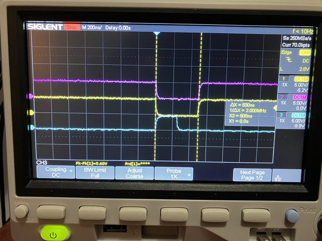
Writing to NIC at IO3-7 always writes a 9F. Read works fine.

Get help from the community & developers with the X16 hardware if you can't find the solution elsewhere
Post Reply
theory
Posts: 3
Joined: Fri Apr 19, 2024 2:25 am

Hardware Writing to NIC at IO3-7 always writes a 9F. Read works fine.

Post by theory »

Hello everyone,

I've been working on a 10/100 NIC for a few weeks now and I almost have it working. For some reason though when I try to write to the card at IO3 ($9f61) or any other IO address, it always writes a $9f to the device. The chip that I am using for the ethernet controller is the Wiznet W5100S. Looking at the timing diagrams of the W5100S and the 65C02 everything appears to be OK even at 8MHz. While I was fairly confident that I was meeting timing requirements I still even tried ANDing the CS with the clock but still the same results; reads just fine but always writes a 9f. I feel like I'm missing something here, which is very possible as I'm fairly new to 65C02 assembly and building hardware for it. I can provide a schematic of the IO select and R/W logic if need be.

The picture below shows the CS (Yellow) WR# (Pink) and D0 (Blue). As you can see, bit 0 is set when the CS and WR signals go low ($9f).
Image

Apologies if this is a newb mistake. Any help would be most appreciated.
Thank you.
kelli217
Posts: 512
Joined: Sun Jul 05, 2020 11:27 pm

Re: Writing to NIC at IO3-7 always writes a 9F. Read works fine.

Post by kelli217 »

Since the upper significant byte of the address for all the IO spaces is $9F, it looks like your hardware is picking up that upper address byte (A8-A15) instead of the actual D0-D7 lines. Double-check your signal routing on the PCB, and the card slot pinout?
theory
Posts: 3
Joined: Fri Apr 19, 2024 2:25 am

Re: Writing to NIC at IO3-7 always writes a 9F. Read works fine.

Post by theory »

I appreciate your response Kelli. I don't think that is it though as I can read the correct data from the device. I just can't seem to write anything other $9f to it. Somehow the KERNAL knows when IO is present (I still haven't wrapped my head around how it does this). For instance, if I don't have the card in a slot and I try to read from say $9f60, I will get a $9f back. If the card is in and I have the jumper set to IO3, I will get the correct value from the device at his MODE register address ($9f60) which is $03.

Here is a schematic of the IOSEL logic and RW/WR signals:
Image

Here is the code that I wrote to read and write to the device:

Code: Select all

CHROUT = $ffd2
NEWLINE = $0d
; Base Address and offsets
IO3START = $9f60		; Base address (MODE Register)
RADDRMSB = $01		; Address pointer MSB
RADDRLSB = $02		; Address pointer LSB
RDATA = $03			; Data register

RRTR = $0017		; Retry TX time register (0x07d0) default value

start:
	lda IO3START
	cmp #$03
	bne fail
	lda #>RRTR
	ldx #<RRTR
	sta IO3START+RADDRMSB
	stx IO3START+RADDRLSB
	lda #$07^$d0
	eor IO3START+RDATA
	eor IO3START+RDATA	; Pointer register auto increments
	bne fail
	bra success
fail:
	lda #1
	jsr CHROUT
	lda #NEWLINE
	jsr CHROUT
	rts

success:
	lda #0
	jsr CHROUT
	lda #NEWLINE
	jsr CHROUT
	rts
Thanks again for the reply.
DragWx
Posts: 304
Joined: Tue Mar 07, 2023 9:07 pm

Re: Writing to NIC at IO3-7 always writes a 9F. Read works fine.

Post by DragWx »

theory wrote: Sat Apr 20, 2024 2:42 am Somehow the KERNAL knows when IO is present (I still haven't wrapped my head around how it does this). For instance, if I don't have the card in a slot and I try to read from say $9f60, I will get a $9f back. If the card is in and I have the jumper set to IO3, I will get the correct value from the device at his MODE register address ($9f60) which is $03.
What's happening here is called "open bus".

Let's say you have LDA $9F60. This translates to the bytes AD 60 9F. When encountering this opcode, the CPU reads AD at address PC, then reads 60 at PC+1, then 9F at PC+2, then finally reads address 9F60.

...but reading 9F60 doesn't go to ROM or RAM, so if there isn't anything to drive the bus when that address is being accessed, the value 9F will still be lingering on the data lines because of bus capacitance.


As for what's wrong when writing, I'm making a guess here, but please look at page 26 of the 65C02 datasheet (the general timing diagram).

There's a timing difference between the "read data" and the "write data" lanes. "Read data" seems to be available on the rising edge of PHI2, but "write data" is not and requires more of a delay. If this is indeed the issue, then I can't provide any advice because I don't know anything about hardware design. :P
theory
Posts: 3
Joined: Fri Apr 19, 2024 2:25 am

Re: Writing to NIC at IO3-7 always writes a 9F. Read works fine.

Post by theory »

DragWx wrote: Sat Apr 20, 2024 7:16 am the value 9F will still be lingering on the data lines because of bus capacitance.
I was wondering if that was it or if the KERNAL was doing it. That makes sense. I'm going to look even closer at the signals on the scope and see if I missed something on the write cycle. Thank you. I really appreciate the the response.
Wavicle
Posts: 268
Joined: Sun Feb 21, 2021 2:40 am

Re: Writing to NIC at IO3-7 always writes a 9F. Read works fine.

Post by Wavicle »

theory wrote: Sat Apr 20, 2024 2:42 am I appreciate your response Kelli. I don't think that is it though as I can read the correct data from the device. I just can't seem to write anything other $9f to it. Somehow the KERNAL knows when IO is present (I still haven't wrapped my head around how it does this). For instance, if I don't have the card in a slot and I try to read from say $9f60, I will get a $9f back. If the card is in and I have the jumper set to IO3, I will get the correct value from the device at his MODE register address ($9f60) which is $03.

Here is a schematic of the IOSEL logic and RW/WR signals:
Image

Here is the code that I wrote to read and write to the device:

Code: Select all

CHROUT = $ffd2
NEWLINE = $0d
; Base Address and offsets
IO3START = $9f60		; Base address (MODE Register)
RADDRMSB = $01		; Address pointer MSB
RADDRLSB = $02		; Address pointer LSB
RDATA = $03			; Data register

RRTR = $0017		; Retry TX time register (0x07d0) default value

start:
	lda IO3START
	cmp #$03
	bne fail
	lda #>RRTR
	ldx #<RRTR
	sta IO3START+RADDRMSB
	stx IO3START+RADDRLSB
	lda #$07^$d0
	eor IO3START+RDATA
	eor IO3START+RDATA	; Pointer register auto increments
	bne fail
	bra success
fail:
	lda #1
	jsr CHROUT
	lda #NEWLINE
	jsr CHROUT
	rts

success:
	lda #0
	jsr CHROUT
	lda #NEWLINE
	jsr CHROUT
	rts
Thanks again for the reply.
Your RD# and WR# signals need to be synchronized with PHI2. According to the W5100S datasheet, the parallel bus is sampled when WR# the signal goes low. During a write by the 65C02, the data is not valid until well after RWB goes low.
65C02_Write_Timing.png
65C02_Write_Timing.png (61.03 KiB) Viewed 210 times
You want to latch the write value on the rising edge of PHI2.
BruceRMcF
Posts: 222
Joined: Sat Jan 07, 2023 10:33 pm

Re: Writing to NIC at IO3-7 always writes a 9F. Read works fine.

Post by BruceRMcF »

Wavicle wrote: Tue Apr 23, 2024 7:12 am... Your RD# and WR# signals need to be synchronized with PHI2. According to the W5100S datasheet, the parallel bus is sampled when WR# the signal goes low. During a write by the 65C02, the data is not valid until well after RWB goes low.

65C02_Write_Timing.png

You want to latch the write value on the rising edge of PHI2.
And the previous discussion suggests one reason why it may be $9F ... the $95 was on the data bus in the previous cycle, so where the datasheet says "write data invalid", it just so happens that the previous state of the data bus from the read of the high byte address byte in the three byte instruction is still on the data lines.

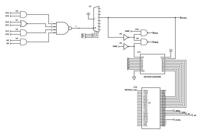
If the system clock is 100Mhz, the WIZnet chip /write_enable cycle time is a minimum of 40ns (4 system clocks), and the address setup time is 10ns (1 system clock). Both the /WIZ_read and /WIZ_write are a minimum of 1 system clock address set-up with a minimum of 2 system clocks set-up on write to the /WIZ and and a maximum data set-up time of 3 system clocks + 5ns for read from the WIZ.

At +5v, the 6502 bus read cycle has a 10ns set-up time before PHI2 drops and a 10ns hold time after PHI2 drops, and valid data will be available from the WIZ chip for reading 45ns after the later of dropping /CS or /Read_Enable , and remain available until /Read_Enable rises. That is much earlier than the 65C02 bus needs it 10ns before PHI2 falls, and with your circuit the RD# rises with a couple of gate delays after /CS rises on the change of the address bus, satisfying the 6502 bus minimum 10ns hold time.

But if the /CS is not qualified on PHI2=1, then the chip select and write enable is generated as fast as that circuit can generate it, and the data to be written to the WIZ chip must be available 40ns after your IOSELECT goes high and WR# goes low.

If the /WE (your WR#) is qualified by PHI2, I am wondering whether you might be OK.

If you switched to a 2-4 decoder (eg, one side of a 74AC139) to generate WR# and RD#, that might do the job. Supposing you are using side 1, /E1 would be the inverse of your IOSEL, 1A0 would be R/W, and 1A1 would be PHI2, with 1Y2 being WR# and 1Y3 being RD#. Then the addressing and the data to be written to the WIZ chip does not have to be available until 40ns after PHI1 rises, which is well after the tMDS of a maximum of 25ns.

Note that you can use the second half of the decode to invert PHI2 by grounding /E2 and 2A1 and tying 2A0 to PHI1, so that 2Y1 is /PHI1 because %01 -> /Active_Low .(maybe dropping both inverters from your RD# and WR# generation allows you to drop from an octal inverter to a hex inverter).
Wavicle
Posts: 268
Joined: Sun Feb 21, 2021 2:40 am

Re: Writing to NIC at IO3-7 always writes a 9F. Read works fine.

Post by Wavicle »

The $9F is written because that was the last value on the bus when RWB went low. The analyzer capture below shows roughly what is going on. In this case the instruction is STA $9F20 ($8D $20 $9f). The markers show that $9F was still on the bus when RWB went low and the value being written ($2A) is driven onto the bus by the CPU 65ns later.
VERA_Write_Capture.png
VERA_Write_Capture.png (113.46 KiB) Viewed 147 times
The glitch on RWB is because of a bug on the early dev boards. This capture is part of the kernel polling for VERA to come out of reset.

Edit for those curious: the time between PHI2 rising edge and $2A appearing on the bus (aka t_MDS) is 35ns. Given the 5ns resolution of the analyzer and the capacitances of the trace and probes, this aligns reasonably to the 25ns published in the datasheet.
BruceRMcF
Posts: 222
Joined: Sat Jan 07, 2023 10:33 pm

Re: Writing to NIC at IO3-7 always writes a 9F. Read works fine.

Post by BruceRMcF »

Wavicle wrote: Tue Apr 23, 2024 7:35 pm ... Edit for those curious: the time between PHI2 rising edge and $2A appearing on the bus (aka t_MDS) is 35ns. Given the 5ns resolution of the analyzer and the capacitances of the trace and probes, this aligns reasonably to the 25ns published in the datasheet.
Yeah, simply qualifying the WR# and RD# lines by PHI1=1 might not fix the issue -- at least, if the qualification is completed too quickly:
WIZ_write_timing.jpg
WIZ_write_timing.jpg (43.84 KiB) Viewed 124 times
... since T_ADDR is 1 system clock -- 10ns at the default 100MHz system clock (40ns if the system clock is set to 25MHz slow mode) and T_DATA is 2 system clocks -- 20ns. The timing diagram is not explicit whether the data acquisition is immediately after the address resolution or if it happens at the end of the write time, with T_DATA being a setup time, but since the timing is counted by system clock cycles, I suspect the first, in which case valid data is required within 10ns of WR# going low.

Actually, come to think of it, using both sides of a 74HC139 might give enough delay. They have a typical delay of 11ns on address changes and 10ns on enable changes, so rather than inverting IOSELECT, IOSELECT could be used as an address line with R/W and the second side of the decoder used to invert PHI2 for the /E1 for the first side:

/DECODE_E1 := DECODE_2Y
DECODE_1A0 := SYSTEM_R/W
DECODE_1A1 := IOSELECT
DECODE_1Y0 =: DNC
DECODE_1Y1 =: DNC
DECODE_1Y2 =: WR#
DECODE_1Y3 =: RD#

/DECODE_E2 := SYSTEM_GND
DECODE_2A0 := SYSTEM_GND
DECODE_2A1 := SYSTEM_PHI1
DECODE_2Y0 =: DNC
DECODE_2Y1 =: DNC
DECODE_2Y2 =: /DECODE_E1
DECODE_2Y3 =: DNC

Between the decoder delays and T_addr, that might be enough delay on the WR# line so that data is valid when T_DATA starts. A more precisely timed delay would be better, but that might have a shot at working.
Post Reply